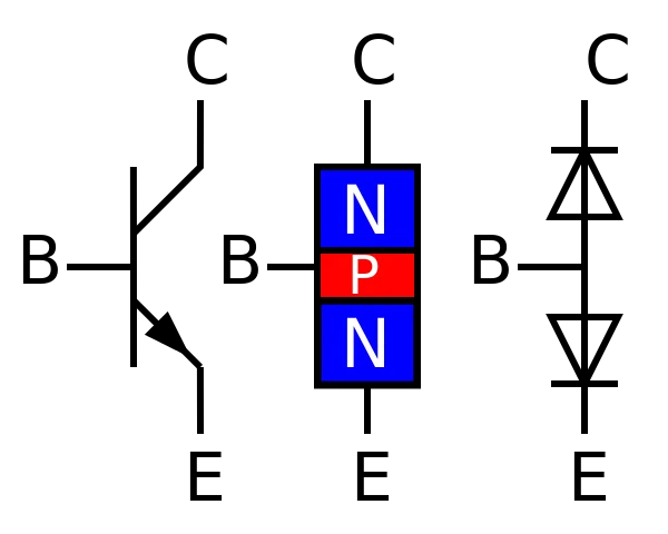
A Bipolar junction transistor, commonly known as BJT, is a Si or Ge semiconductor device that is structured like two p-n junction diodes connected back to back. It has two outer regions which are the emitter and collector and another region in the middle known as the base. The bipolar junction transistor is called bipolar as both holes and electrons play a fundamental role in its operation.
BJT is a current controlled device, meaning that the current flow through the collector and emitter is controlled by the magnitude of current flowing into the base.
- Symbol and terminals in bipolar junction transistor
- Types of Bipolar Junction Transistor and their Operation
- NPN Transistor
- PNP transistor
- Working principle of BJT
- Transport factor
- Current gain
- Operation regions of BJT
- Bipolar Junction Transistor Circuits Configurations and Characteristics
- Bipolar Junction Transistors as a Switch
- Advantages and Disadvantages of Bipolar Junction Transistor
- Review
Symbol and terminals in bipolar junction transistor
Emitter: A heavily dope region, that passes charged particles to the base.
Base: A thin and lightly dope region. Base passes the charged particles from the emitter to the collector.
Collector: The largest region of a transistor. It is lightly doped than the emitter but heavily doped than the base. Bipolar junction transistors aid in regulating the current flow in a circuit. The current that flows through the transistor is in proportion to the amount of biasing voltage that is being applied at the base terminal.
Types of Bipolar Junction Transistor and their Operation
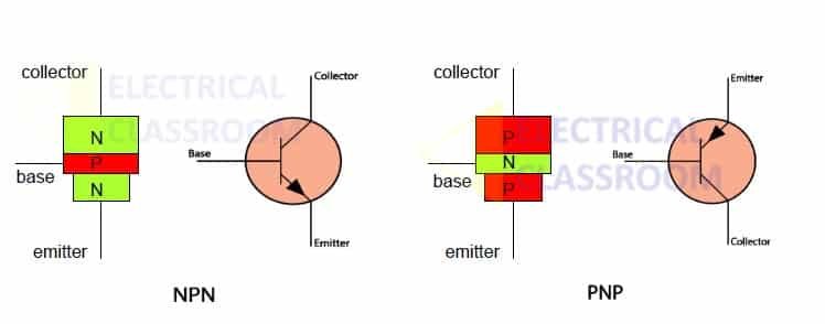
Based on their construction, there are two types of BJTs which are the P-N-P and N-P-N types. These two types of structures operate in a similar way. The only difference is their biasing and the polarity of the power supply for each of the structures. The N-type has extra electrons added to it which causes it to become negative. The P-type has electrons removed from it which result in the formation of holes, therefore giving it a positive charge.
NPN Transistor
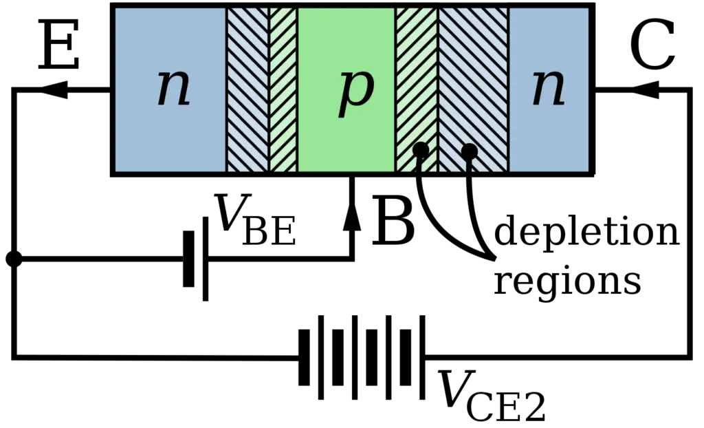
The N-P-N transistors consist of two N- doped semiconductor layers which act as the emitter and collector and a single P-doped layer which acts as the base. A high current is produced in the collector and emitter when the current at the base is amplified. (Elprocus, n.d.)
IE, IB and IC are the emitter and collector current and VEB and VCB are the emitter-base and collector base voltages. According to the sign convention, it can be observed that when the current flows into all the terminals the sign of the current is positive. When the current flows out of the emitter terminal and exits the transistor the sign of the current is negative.
A bipolar junction transistor is that it works as an electron valve. When there is no current flowing in the transistor this is because the p-type silicon semiconductor does not have enough electrons which act as a barrier for the conduction of current to take place. The N-P-N bipolar junction transistor will only work when the electrons flow from a region of low electron junction to an area of high electron junction.
An NPN transistor is considered to be in its ON state when the minority carriers in the P-type region allows the electrons to flow between the collector and emitter terminals of the transistor. This allows a large amount of current to flow in the circuit, therefore resulting in faster operation.
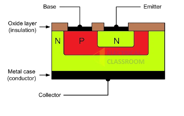
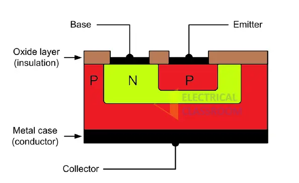
The structure of NPN bipolar junction transistor is shown in the figure. It consists of highly doped N type emitter which is surrounded by a P-type lightly doped base. The collector covers the larger portion of the BJT and surrounds the base and the emitter.
PNP transistor
The P-N-P transistor consists of one N-doped semiconductor layer which is the base and two layers of P-doped semiconductor material which act as the collector and emitter. The amplified base current enters the collector at the output. In the P-N-P the current flow is controlled by the base but the current flow is from emitter to collector.
In the figure above, it can be observed that the current flow is positive from the emitter terminal but leaves negative from the base terminal into the collector terminal and then exits the transistor with a negative sign. Therefore, VEB is positive whereas VCB and VCE are negative as the current flowing through the base and collector junction is negative.
The P-N-P transistor produces a lower current output compared to the N-P-N transistor because instead of electrons, the emitter emits “holes” which denotes the absence of electrons that are collected by the collector. Hence, the transistor operates much slower and is not used as often as the N-P-N transistor.
The structure of PNP bipolar junction transistor is shown in the figure. It consists of highly doped P type emitter which is surrounded by a N-type lightly doped base. The collector covers the larger portion of the BJT and surrounds the base and the emitter.
Working principle of BJT
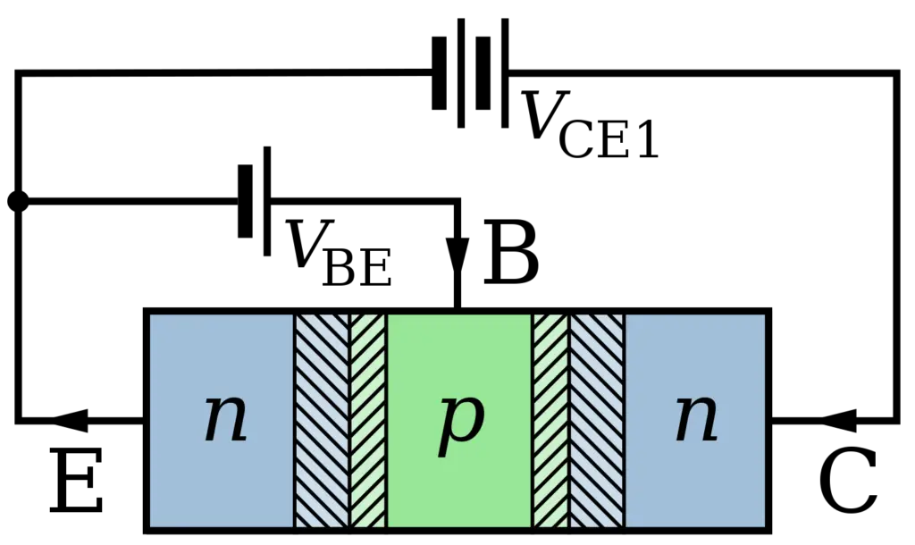
Since the bipolar junction transistors are made by connecting two diodes back to back, there exists quasi-neutral regions in the emitter, base and collector. These regions remain neutral only at a thermal equilibrium state. This is because when a voltage is supplied the charge densities and electric field in these regions do not change significantly compared to the depletion region. Therefore, for calculating the operation of the BJT these regions are considered neutral. In BJT the emitter to the base junction is forward biased and the collector to the base junction is reverse biased.
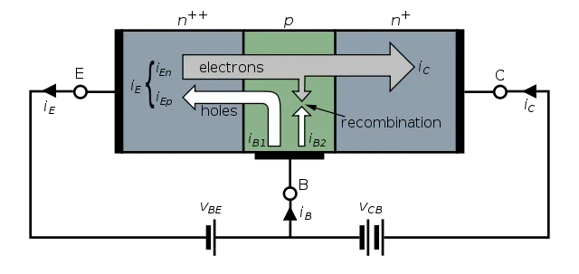
When the required voltage is applied to the base, a certain amount of current flows into the base (IB). This turns on the transistor and which in turn allows current flow from the collector to the emitter (Assuming that the transistor is NPN type). Let us assume that the base-emitter junction is forward-biased and the base-collector junction is reverse-biased. The following phenomenon occurs inside the transistor:
- Since the base-emitter junction is forward-biased, the positively charged holes from the lightly doped base move through the PN junction to the emitter.
- Also, the forward bias reduces the barrier potential of the base-emitter junction. Hence, a small amount of electrons (nearly 1%) from the emitter crosses the base-emitter junction to reach the lightly doped base and recombines with the holes in the base.
- The remaining electrons in the emitter (about 99%) cross the base-emitter junction and pass through the base-collector junction resulting in electron flow from the emitter to the collector. This constitutes the collector’s current IB.
IE=IC+ IB
A similar phenomenon occurs in the PNP transistor, but the electrons are replaced by holes and holes are replaced by electrons.
Transport factor
The ratio between the collector and emitter current is called the transport factor.
Current gain
The ratio between the collector and base current is known as the current gain.
Operation regions of BJT
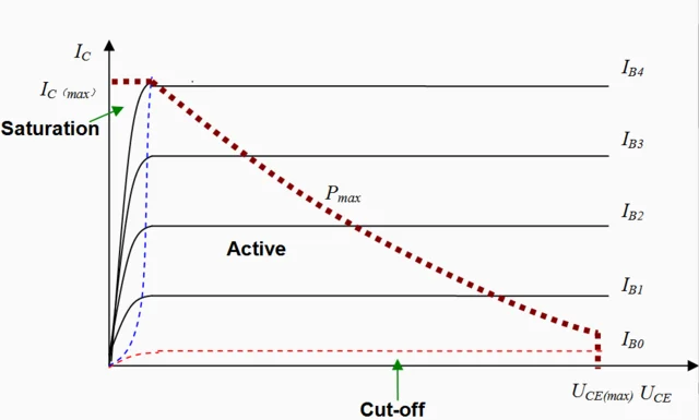
BJT can act as either insulators or conductors depending on the base current. This gives them the ability to change between two varying states that are switching and amplification. Therefore, the BJT can operate in three operational modes which are:
- Active region: – When the transistor operates in the active region it acts as an amplifier where Ic = β.Ib
- Saturation region: – In this region, the transistor is in a full “ON state” and operates as a switch. Here the collector current is equivalent to the saturation current.
- Cut-Off region: – In the cut-off region the transistor in a full “OFF state” and operates as a switch. No collector current flows through the circuit.
The controlled current flows between the emitter and collector and the controlling current flow to the base. Therefore, a small base current controls the larger collector current. When the base has no current flowing through it then it is in a cut-off state. When the transistor has maximum current flowing through it then it is said to be in the saturation region and is in a fully conducting state.
Bipolar Junction Transistor Circuits Configurations and Characteristics
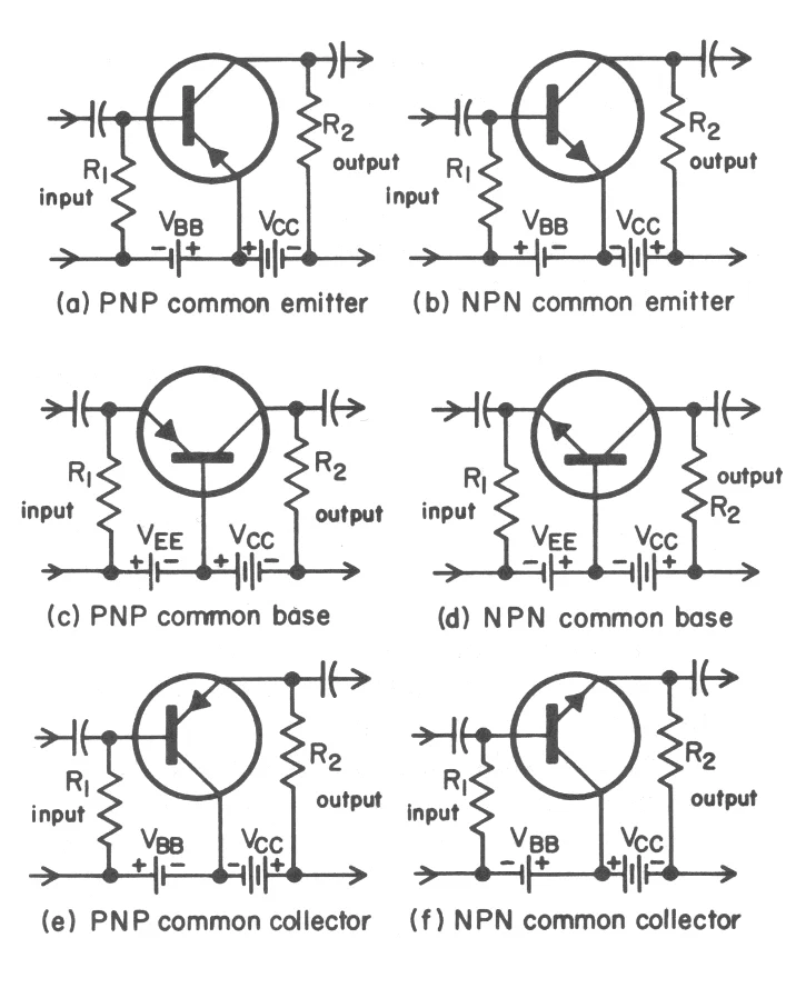
The bipolar junction transistor has three basic circuit configurations that can be used. They are: –
- Common Emitter Circuit – In the emitter-collector configuration, the emitter remains common while the base acts as the input and the collector acts as the output.
- Common Base circuit – In the common-base configuration, the base remains common while the emitter acts as input and the collector acts as the output.
- Common Collector Circuit – In the common-collector configuration, the collector remains common while the base acts as the input and the emitter acts as the output.
| Characteristic | Common Base | Common Emitter | Common Collector |
|---|---|---|---|
| Input Impedance | Low | Medium | High |
| Output Impedance | Very High | High | Low |
| Phase Shift | 0o | 180o | 0o |
| Voltage Gain | High | Medium | Low |
| Current Gain | Low | Medium | High |
| Power Gain | Low | Very High | Medium |
The transistor’s characteristics are expressed via the voltage and current relationship. These circuit configurations have varying characteristics which can be analyzed by the following characteristic curves:
- Input characteristics curve describes the changes in the value of the input current with respect to the input voltages and the output voltage is kept constant.
- The output characteristics curve is plotted against the output current and output voltage where the input current is kept constant.
- The transfer characteristic curve explains the variation of the output current with respect to the input current where the output voltage is kept constant.
Bipolar Junction Transistors as a Switch
By controlling the base current, the emitter resistance can become either nearly infinite or zero. For a BJT to operate as a switch, the overall resistance across the BJT should be either zero or very negligible. To achieve this the P-N-P or N-P-N BJT needs to operate within the cut-off and saturation region. Here is a simple example of BJT as a switch.

Advantages and Disadvantages of Bipolar Junction Transistor
Here is a list of advantages of using Bipolar Junction Transistors:
- The voltage gain is much better than MOSFET
- BJT has a low forward voltage
- It can be operated in a wide range of low to high power applications
- It shows better performance at high frequency and has a large gain bandwidths
- BJT has a high current density
The list of disadvantages of using BJT are:
- They produce more noise
- They have low thermal stability
- The switching frequency of a BJT is low
- It requires a lot of attention as the switching time is not very fast compared to the high alternating current and voltage frequencies. This can lead to confusion, therefore, providing complex control over the base.
Download: Sample datasheet of a bipolar junction transistor
Review
- Bipolar junction transistors or BJT is a semiconductor device that is structured like two p-n junction diodes connected back to back.
- The three leads of a BJT are Collector, base, and emitter.
- Two types of BJT are NPN and PNP.
- A Bipolar Junction transistor is a current-controlled device.
- The amount of current flow between the collector and the emitter is determined by the base current.
- When zero current flows through the BJT it is said to be at the cutoff state and when maximum current flows through it, it is said to be at a saturation state. This property facilitates its usage as an ON/OFF switch.
- The state between the cutoff state and the saturation state is known as the active state.

thank you, nice explanation.
simple and complete.
best wishes.