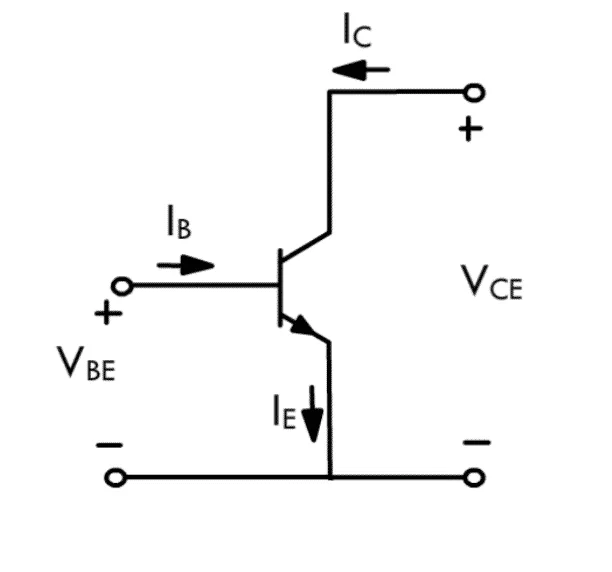
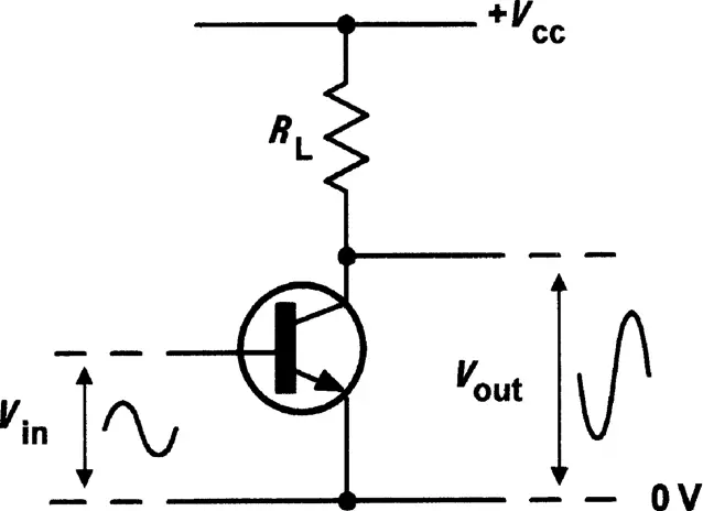
The common emitter circuit is probably the most widely used transistor configuration. The emitter electrode is common to both input and output circuits. The common emitter amplifier has a typical input impedance of 1kilo ohms and a typical output impedance of 10 kilo-ohms. Also, the output will be the inverse of the input, which means the output experiences a 180° phase change. This results in a remarkable overall performance.
Operation of common emitter amplier
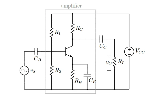
The common emitter amplifier circuit comprises of a voltage divider bias and coupling capacitor CB and CC at the input and output and a bypass capacitor CE which is connected from the emitter to the ground. The capacitor CB couples the input signal to the input port of the amplifier. It also separates the AC signals from the DC biasing voltage.
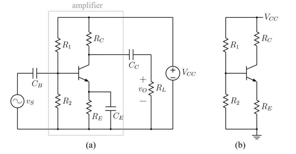
The capacitor CC couples the output signal to the load resistance RL. This is because an AC input signal is applied at the base and then taken from the collector terminal as the output signal. Both the input and output signals have the emitter as a common terminal.
The bypass capacitor CC shorts the signal at the emitter to the ground, therefore, ensuring that no signal flows through the emitter at a particular frequency. This is done to supply base bias voltage. That is why the amplified output signal is 180̊ out of phase of the input signal.
The voltage divider biasing has two resistors (R1 and R2) which are connected midpoint to the base terminal of the transistor. This forms a potential divider which supplies the base with voltage bias. R1 resistor is used to produce the forward bias voltage and R2 is used to ensure that a bias voltage is developed.
The thermal stability of the amplifier is regulated through the resistor RE at the emitter terminal connection. R1, R2 and RE are extremely important for the stabilization of the circuit and the formation of the bias voltage. If these resistors fail to perform, a proper operating point would not be established. This could result in the negative half-cycle being cut off from the output signal.
Phase shift
Phase shift is the phase angle between the input and amplified output signal measured in degrees is known as phase shift. The conventional single-stage amplifiers provide a phase shift of either 180o or 360o.
DC Analysis of CE Amplifier
The common emitter amplifier operates when an AC input signal flows through the emitter-base junction. The input signals alternate between positive and negative peak values. The signal is in a forward bias direction and increases when it moves across the junction during the upper half cycle.
The collector current also increases significantly due to an increase in the flow of electrons from the emitter to the collector through the base. The current also increases across the collector load resistor RC and a voltage drop is also observed across the collector. Therefore, the overall output signal is amplified. This shows that in the upper half of the cycle the common-emitter circuit is amplifying the input signal.
While the upper half cycle increases the forward bias voltage, the lower half cycle decreases the forward bias voltage across the emitter-base junction. Therefore, the decreased collector-base voltage causes the collector current to be reduced across the collector load resistance RC. This is how we obtain the full cycle of the forward bias voltage.
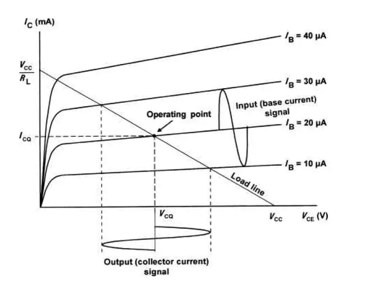
This process of making the negative and positive peak values is achieved through the process of biasing. Biasing is very important for amplifier designs as it helps establish the operating point of the transistor amplifier at which it would receive signals. This way, the distortions in the output signal of the amplifier are greatly reduced as the proper parameters of the most efficient operating conditions are established. Bias refers to the DC current and voltage inside the amplifier circuit.
Under DC conditions all the three capacitors (CB, CE and CC) in the common emitter amplifier are replaced with open circuits. The transistor gain β is assumed to be very large such that it goes to infinity. Due to this assumption the base current can be neglected. This way the R1-R2 network operates as a voltage divider. The transistor bias voltage is calculated by:
VCC is the supply voltage that also aids in determining the maximum collector current, IC when the transistor is fully switched ON, VCE = 0.
To operate as an amplifier, the BJT needs to operate within the active region. The base-emitter junction should be in forward bias and the base-collector junction needs to be under reverse bias. The base-emitter voltage drop can be recorded by:
At first, we sample in the
(
is odd) equidistant points around
:
For a silicon BJT, the difference between these voltages gives a voltage drop of about 0.7V. Hence, through this value, the VE can be recorded as:
The emitter current IE is:
The collector current is assumed to be equivalent to the IC because it is assumed the gain of the transistor amplifier is very large. The current gain, of the common emitter amplifier is the ratio of the change in the collector current to the change in the base current. The voltage gain,
in the product of the current gain and the ratio of the output collector resistance to the input resistance of the base circuits. Hence the following equations define the current gain and the voltage gain.
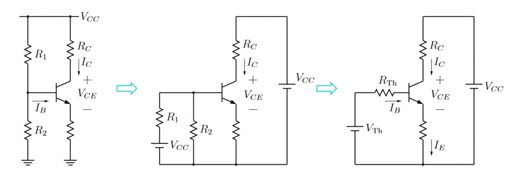
The base current IB can be calculated using the Thevenin equivalent circuit. It is found by the collector current IC and the DC current gain β. The Kirchhoff voltage loop in the Base to Emitter loop can be represented as:
Where RTh represent the parallel resistance between R1 and R2 and VTh= VB .
These calculations sum up the DC analysis of the collector-emitter amplifier.
AC analysis of CE Amplifier
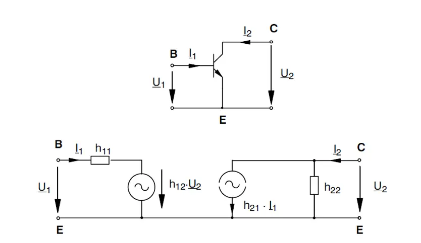
To calculate the alternating current behaviour of transistor circuits, substitute circuit diagrams are often used that show the transistor with regards to its terminal behaviour. There are a large number of equivalent circuit diagrams, however, the h-parameter equivalent circuit diagram is preferred to calculate circuits with bipolar transistors.
‘h’ parameters are four parameters that describe the behaviour of a two-port network system. This linear network is formed when the resistance, inductance, capacitance remain fixed and only the voltage across them changes. Therefore, these parameters are divided into h11, h12, h21 and h22 where the first subscript number denotes the input variable and the second denotes the output variable. It is in a subscript form which means the first number is always divided by the second number. ‘h’ parameters are also known as hybrid parameters as they are a mixture of two variables.
The equations resulting from this equivalent circuit are as follows: –
The h parameters can be easily determined and are measured by the parameter values which are different as they depend on which pair of terminals are viewed as input or output. Where:
- h11 is the input resistance.
- h12 is the input resistance.
- h21 is the input resistance.
- h22 is the input resistance.
In the case of high frequencies, capacities between the base-emitter, base-collector and collector-emitter connections must also be taken into account in the equivalent circuit diagram. This also includes the base-collector resistor, which however is neglected in most cases because it is very large. The capacitances determine the cut-off frequencies of the basic transistor circuits. This type of circuit is suitable for lab testing as the capacities produce negligible frequencies.
Characteristics of Common Emitter Amplifier
A few notable characteristics of the common emitter amplifier are:
- The common emitter amplifier has a high power gain.
- The input and output have a phase relationship of 180 degrees.
- It has a medium voltage gain.
Various characteristics of Common emitter configuration of BJT
| Parameter | Values |
|---|---|
| Voltage gain | Medium – typically 40 |
| Current Gain | High – typically 200 |
| Power gain | Very High – typically 8000 |
| Input resistance | Medium – 2.5kΩ |
| Output resistance | High – 20kΩ |
| Phase shift | 1800 |
| Typical application | General Purpose AF and RF amplifiers |
Pros and Cons of Using the Common Emitter Amplifier Configuration
Advantages
A few advantages of using the common emitter amplifier are:
- The output impedance of the amplifier is high.
- The input impedance is low and it works as an inverting amplifier
- It has medium voltage and high current gain which results in a high power gain.
Disadvantages
A few disadvantages of using the common emitter amplifier are:
- The common emitter amplifier does not respond to high frequencies.
- The voltage gain of the amplifier is not stable.
- It has a very high output resistance.
- Despite the presence of resistors, there are still chances of thermal instability in the circuit.
Nowadays common-emitter amplifiers are being used in applications that require low-frequency voltage and noise amplifiers. Radiofrequency transceiver circuits also make use of common-emitter amplifiers.
