A gate turn-off thyristor (GTO) is three terminal semiconductor device – made up of four layers of alternating P-type and N-type material. Just like a conventional thyristor, it is also a current controlled, minority carrier device. The gate turn-off thyristor was invented with the purpose to address the difficulties in the turn OFF mechanism of silicon controller rectifiers (SCRs). It functions similarly to the conventional thyristor except for the turn-off function.
Symbol of GTO
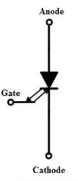
The symbol of the GTO is shown in the picture. It differs from the conventional thyristor(SCR) such that it can be turned OFF by applying a negative gate signal. This is where the thyristor gets its name from. It can be observed from the symbol the gate terminal has double arrows indicating the bi-directional flow of current through the gate terminal.
The GTO is triggered into conduction by a small gate current and it can be switched off by a very high negative gate current pulse. In the ON state, it behaves like a conventional thyristor. Unlike the normal thyristor, the switching speed is much faster for the GTO and it also has much higher current and voltage ratings compared to power transistors.
GTO thyristors with forward and reverse blocking capabilities are known as symmetric GTOs. These are used in current source inverters but are slower compared to asymmetric GTOs. Asymmetric GTOs are commonly used due to a lower ON-state voltage drop and relatively safer and stable temperature characteristics. They have high reverse voltage capabilities. They are used in circuits when no reverse voltage pass through them or a reverse conducting diode is connected in the circuit.
Structure of Gate turn-off thyristors
The thyristor needs to maintain a high emitter efficiency at the cathode where the n+ cathode is heavily doped. The breakdown voltage at junction 3 is also low. To maintain the emitter efficiency, the doping layer of the p-type gate region must be kept low. This increases the emitter efficiency but reduces the efficiency of the turn-off function which requires the resistivity of this region to be low and the doping to be high. As this device’s primary mechanism is its turn OFF characteristic this region is kept highly doped. Also, the gate cathode junction is kept highly interdigitated to improve the current turn of capabilities at this junction.
A GTO thyristor consists of multiple segments which are arranged in concentric rings around the center of the device. The thickness and doping level of the n-type base region determines the maximum forward-blocking voltage of the device. The doping level is kept low to block high levels of forwarding voltage and thickness is kept higher possibly about a few hundred microns.
If the voltage flows beyond the maximum threshold of the forward voltage then the electric field at junction 2 which is the main junction can exceed its critical value and avalanche breakdown can occur. Secondly, it can also result in fully depleting the n base. This would result in the electric field punching through the anode emitter. The anode junction (J1) is the junction between the n-base and p+ anode. The efficiency of the anode junction should be kept as high as possible to ensure good turn ON properties. This would require the p+ anode region of this junction to be highly doped.
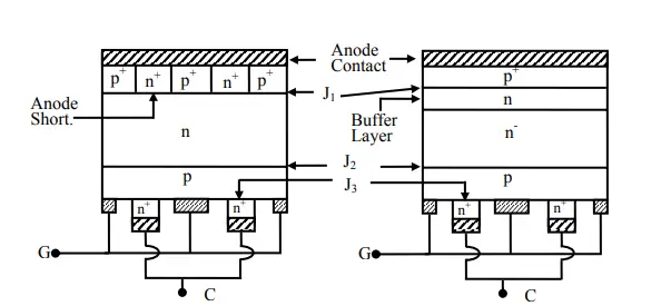
While the turn ON properties of the GTO is efficient the turn OFF properties for this type of GTO are relatively poor. It results in high losses and the maximum turn-off current is very low. To solve this problem two types of approaches are taken one is the anode shorted GTO and the second is the Buffer GTO.
Types of GTO
Anode Shorted GTO
For this type of method, heavily doped n+ layers are introduced into the p+ anode layer. It can be observed in the figure that the layers make contact with the anode metallic contact which causes the electrons traveling through the base to directly reach the anode metal contact. This prevents hole injection to take place from the p+ anode. The addition of these anode shorts reduces the reverse voltage blocking capacity of the GTO to the reverse breakdown voltage of junction J3.
The more the amount of anode shorts the lower the efficiency of the anode junction. This lowers the turn ON efficiency of the device and increases the turn OFF efficiency. Also, the density of the anode shorts needs to be carefully chosen so that a proper performance line can be drawn between the turn ON and turn OFF performance of the device. The anode-shorted structure is very commonly used.
Buffer Layer GTO
The buffer layer structure has a much soberly doped n-type buffer layer that is put between the n-type base and anode. This causes the electrical field patterns formed in the n-base region to change in the shape from triangular to trapezoid and also reduces the width of the electric field. This results in increasing the device’s efficiency for the turn OFF mechanism.
Operation of the GTO
In the ON state, the central base regions of the GTO thyristor get filled with holes that are supplied from the anode and the electrons are supplied from the cathode. Holes can be extracted from the gate by applying a reverse bias. This would make the gate negative with respect to the cathode and suppress the injection of cathodes.
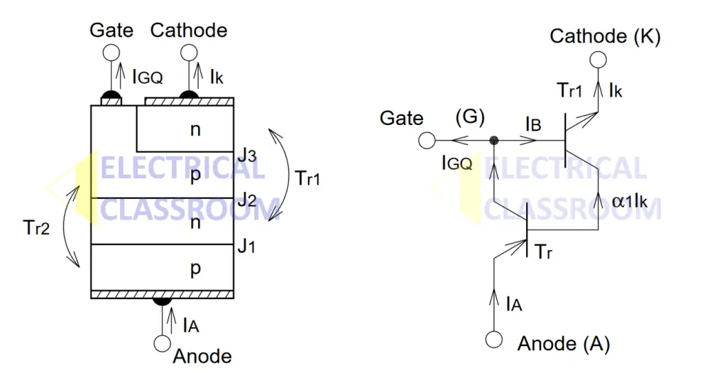
More holes are then extracted from the gate due to this suppression which results in further suppression of electron injection. This puts the cathode emitter junction into a complete reverse bias state and switches it OFF. This can be observed in figure 3 which shows the two-transistor model for the turn-off operation.
Referring to the two-transistor model, the GTO thyristor is divided into NPN transistor Tr1 and PNP transistor Tr2. Tr1 is on the cathode end and Tr2 is on the anode end. When a reverse current flows through the IGQ flows through the gate, the base current IB at the transistor Tr1 would be reduced as the IGQ increases.
The electron current IRB disappears due to the recombination in the Tr1 base layer. The anode current (IA) is the sum of the gate current IGQ and the cathode current (IK). To turn the thyristor off the base current needs to be smaller than the IRB. In theory, if an adequate amount of reverse bias current is supplied to the gate, then the turn-off function will automatically be carried out by the GTO thyristor.
Advantages of a GTO over conventional thyristor
The gate turn-off thyristors have the following advantages over conventional thyristors:
- They have excellent switching characteristics such that they outperform conventional thyristors in their high-frequency characteristics and efficiency.
- They do not require a separate commutation circuit.
- Lack of commutation circuit results in the reduction of noise generation and electromagnetic waves.
Applications
- They are used in pulse width modulation inverter systems in the PWM converter and inverter.
- DC choppers and drives
- They are used in variable frequency drives and soft starters.
- Induction heating equipment
- Power supplies that require AC stabilization.
- DC circuit breakers.


