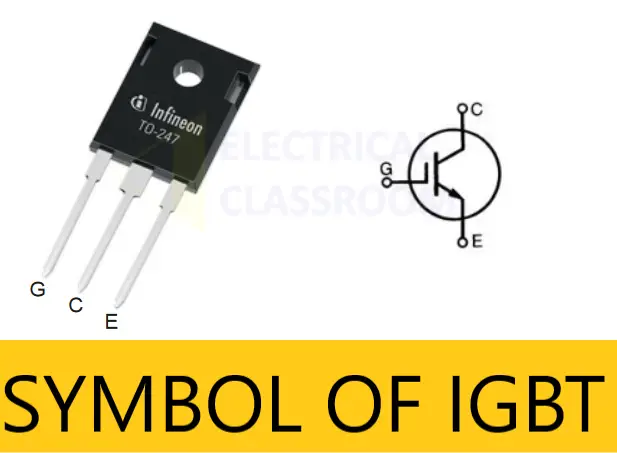
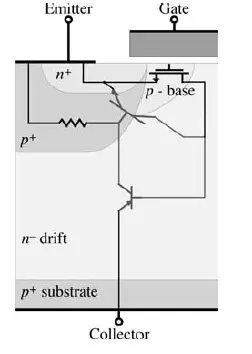
An insulated-gate bipolar transistor (IGBT) is a type of bipolar transistor that has an insulated gate terminal. The structure of the IGBT includes an input MOSFET which consists of the gate terminal and the output BJT consists of the collector and emitter terminals. The collector and emitter are the conduction terminals and the gate is the control terminal that controls the switching operation.
IGBT is a minority carrier that is preferred for high current or high voltage applications. It has high input impedance and large current carrying capabilities. This is because they are designed to cater to high power applications which have a low power input.
Structure of IGBT
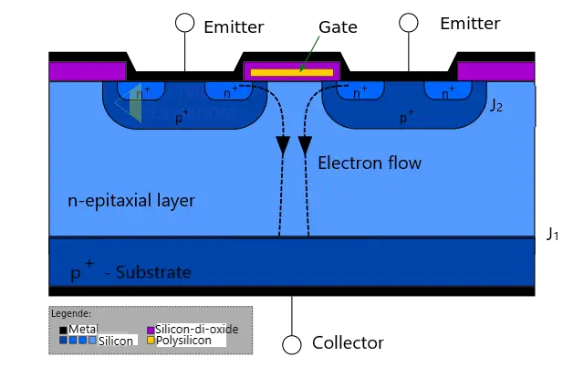
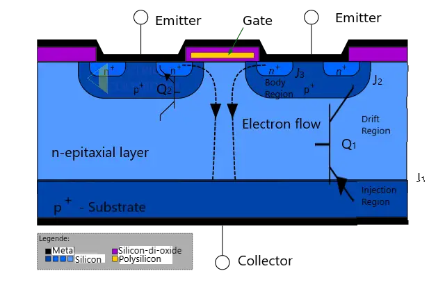
IGBT is made of silicon and is very similar in structure to Power MOSFET. The only difference is that the injection layer is p+ and not n+ substrate as in Power MOSFET. The injection layer is very integral to the characteristics of the IGBT. The other two layers are called the body region (J2) and the drift (J1). The n+ layer at the top of the IGBT is the source or the emitter. The P+ layer at the bottom is the drain or the collector. P-channel IGBT shares a similar structure to the N-channel IGBT except the doping is reversed in each layer.
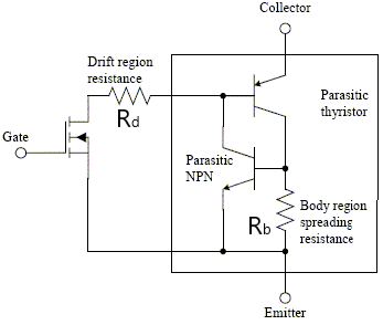
In this structure, it can be observed that it is an n-channel MOSFET and has two bipolar junction transistors (BJT) which are Q1 and Q2. Q1 BJT is a p-n-p transistor and Q2 is an n-p-n BJT. The drift region experiences a resistance which is known as Rd and the resistance offered by the p body region is known as Rb. The collector of Q1 shares the same base as Q2 and the collector of Q2 is the same as the base of Q1.
The collector of the PNP is connected to the base of the NPN transistor whereas the collector and base of the PNP are connected. The arrangement of these transistors forms a parasitic thyristor which creates a negative feedback loop. A parasitic thyristor is formed by the two BJT transistors stacked next to one another.
The base and emitter terminals are connected through the resistor Rb of the NPN transistor. This is done to ensure that the parasitic thyristor doesn’t latch-up which would cause the latching of the IGBT.
Working of the IGBT
The voltage source (VG) is connected to the gate terminal in a positive direction to the emitter and collector. The voltage source (VCC) is connected across the emitter and the collector. The collector is positive to the emitter. Junction J1 is forward biased due to the VCC. The junction J2 is reverse biased and no current will flow inside the IGBT from the collector to the emitter. At the start, no voltage is applied to the gate terminal. Hence, the gate terminal is in a non-conductive state.

Only a small amount of voltage is required for it to go into a conduction state. As the gate voltage is increased, the capacitance effect will take on the silicon dioxide layer which would cause the negative ions to accumulate on the upper layer and the positive ions to accumulate on the lower side of the silicon dioxide layer. This will result in the insertion of the negative charge carriers in the p region.
The accumulation of negative charge carriers will increase as the voltage source at the gate terminal increases. This will allow a channel for the current to the current to flow from the collector to the emitter between the J2 junctions. The current increases as the voltage source (VG) increase.
Types of IGBT
There are two types of IGBT:
- Non-punch Through (NPT) IGBT
- Punch through (PT) IGBT
Non-punch Through (NPT)
The vertical cross-section of a PT IGBT is shown in the figure. It has a p+ substrate at the bottom. This forms a pn-junction with n– drift region. The conduction modulation in this junction occurs by injecting minority carriers into the n– drift region. The p+ substrate, n– drift and the p+ emitter together constitute a BJT. NPT IGBTs are known as symmetrical IGBTs.
Symmetrical IGBTs have a forward and reverse breakdown voltage which is equal in quantity. They are used more widely in AC circuits. The switching loss is medium. It has a long, low amplitude tail current. The conduction loss is also medium and increases as the temperature increases. It has a short circuit rated and paralleling is also easy.
Punch through IGBT
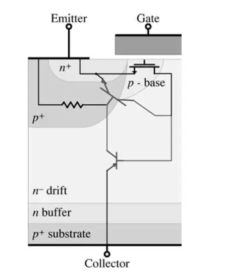
In order to minimize the switching time, a buffer layer is added in the drift region. The buffer layer is heavily doped with n-type material, placed above the p+ substrate. Because of much higher doping density, the injection efficiency of the collector junction and the minority carrier lifetime in the base region is reduced. PT IGBTs are known as assymeterical IGBTs.
The asymmetric IGBTs have a reverse breakdown voltage which is less than the forward breakdown voltage. They are used more widely in DC circuits and do not require any support voltage in the opposite direction. The switching loss of the PT is low and has a short tail current. The conduction loss is low and decreases with temperature. Paralleling is very difficult and the rated short-circuit is limited, therefore, causing a high gain.
Operation Modes
There are two types of operation modes:
- Forward-Blocking Mode
- Conduction Mode
- Reverse-Blocking Mode
Forward-Blocking Mode
Let us consider that the gate terminal is kept at the ground potential and a positive voltage is applied to the collector terminal. This results in the forward bias of the junction between the substrate and the drift region and reverse bias of the junction between the p-base and drift regions. Under this condition, the device enters forward-blocking mode until the base breakdown voltage is reached.
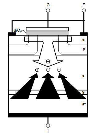
Conduction Mode
When a positive gate voltage is applied to the device, an n-channel is formed in the base region which provides a path for electrons to flow from n+ base to n– drift region. As the junction between the substrate and the base is already in forward bias, holes from the collector move towards the drift region and neutralize the electrons forming a neutral drift region. The remaining holes move towards the emitter causing a vertical current flow.
Reverse-blocking Mode
Let us consider that the emitter is kept at ground potential. When a negative voltage applied to the collector, the junction between the substrate and the drift region is reverse biased. This prevents any current flow in the device and the device enters the reverse blocking mode.
The forward voltage drop increases with increasing width of the N- – drift region width. The width of the N- – drift region also determines the reverse voltage capability. The forward voltage drop can be calculated as follows:
where is Minority carrier diffusion length,
is the maximum blocking voltage and
is the permittivity of free space.
Characteristics of IGBT
The static I-V characteristic graph for the n-channel IGBT is similar to a BJT except the VGE is kept constant because an IGBT is a voltage-controlled device. The device is in an “OFF” state when the voltage across the collector-emitter is positive and the gate–emitter voltage (VGE) is less than the threshold voltage across the gate-emitter (VGET). The reverse voltage is blocked by junction J2 and when the voltage across the collector-emitter is negative, junction J1 blocks the voltage.
Transfer Characteristics
The n-channel IGBT is going to be in an ON state if the VGE is greater than the threshold value VGET.
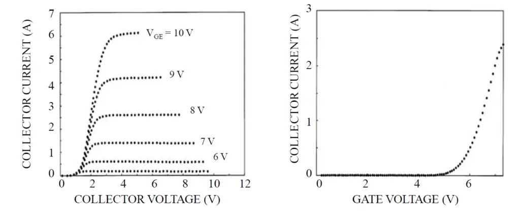
The transfer characteristic is the variation of the current (ICE) flowing through the collector-emitter with the VGE at varying temperature. The gradient of the transfer characteristic at a particular temperature gives the transconductance of the IGBT device.
Switching Characteristics of IGBT
As the IGBT is a voltage-controlled device it only requires a small voltage for the gate to remain in a conduction state. IGBT are unidirectional devices that only switch current in the forward direction, which is from the collector to the emitter. The figure below shows a switching circuit of the IGBT.
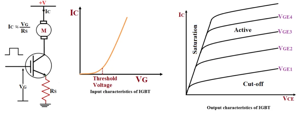
VG is applied to the gate pin which switches the motor (M) from a supply voltage V+. Rs limits the amount of current which flows through the motor.
For the input characteristics when no voltage is applied to the gate pin the IGBT is OFF and no current can flow through the collector pin. For the IGBT device to begin conducting the applied gate pin voltage needs to exceed the threshold voltage. Once that is achieved the IGBT would be in a conduction state and a current (IG) will flow through the collector and emitter terminals. The collector current (IC) and the gate voltage are directly proportional to one another.
The IGBT has three stages in the output characteristics. The VGE is 0 when the device is in an OFF condition and is in the cut-off region. When the voltage at the gate is increased, a small leakage current flows through the device when the VGE is less than the threshold voltage. During this time frame, the device remains in the cut-off region. When VGE exceeds the threshold voltage that is when the device enters the active region and the current is observed to be flowing through the device. The increase in the flow of current is directly proportional to the increase in voltage VGE.
The turn-on time (Ton) of the IGBT consists of two components which is the rise time (tri) and delay time (tdon). The time during which the collector current rises from leakage current ICE to a final collector current of 10% of IC and the collector to emitter voltage falls from VCE to 90% of VCE is known as the delay time. Rise time is the one during which the collector current increases from 10% to 100% of IC and the collector-emitter voltage falls from 90% of VCE to 10% of VCE.
Similarly, the turn off time has three components which are the delay time off (dtf), fall time (tfi). The delay time off takes place when the collector current falls from the IC to 0.9IC and the collector to emitter voltage (VCE) begins to rise.
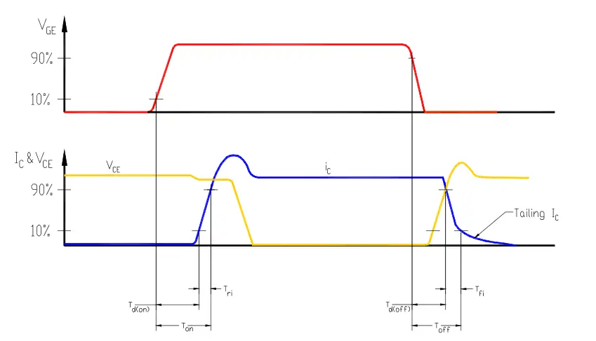
Initial fall time is when the collector current falls from 0.9 IC to 0.2IC and the collector-emitter VCE rise to 0.1. The final fall time occurs when the collector current falls from 0.2 IC to 0.1C and the collector to emitter voltage rises from 0.1 VCE to a final value of VCE.
Losses in IGBT
As like every semiconductor devices, IGBTs have switching and conduction losses.
Conduction loss
Conduction loss occurs in an IGBT when it is in forward conducting mode. Conduction losses can be calculated using the following formula.
Pcond = VCE x IC
Switching loss
Switching losses occurs during turn-on and turn-off. Switching losses depends on the collector current, gate resistance, temperature. Turn-on and turn-off losses can be calculated by multiplying the conduction loss at the time of switching by the switching frequency.
Application
Today, IGBTS are widely used in AC and DC motor drives, Switch-mode power supplies (SMPS), induction heating, Unregulated Power Supply (UPS), inverter, in bipolar power transistors to act as a switch in single devices and it is also used to combine IGFET to control the input.
