What is a diode?
A diode is an electrical component that allows the current to flow in only one particular direction. Diodes are made up of silicon and germanium. They are used to protect the circuit by limiting the voltage and transforming the AC voltage into DC voltage. There are many types of diodes and each diode has its own set of uses.
Symbol of diode
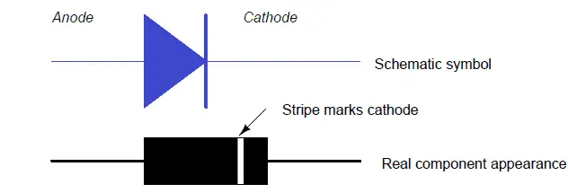
A diode is represented by a triangle adjoining the line. It has two terminals: the anode, which is the positive terminal, and the cathode, which is the negative terminal. The terminal entering the flat edge of the triangle is the anode and the other end is the cathode. The arrow in the diode symbol represents the direction of the conventional current when the diode is in operation.
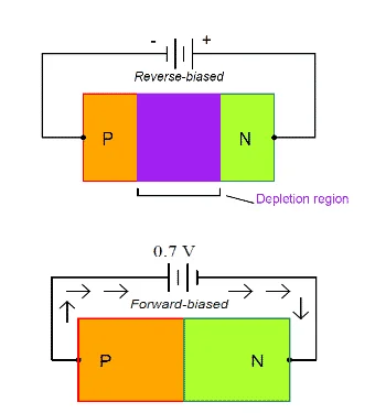
In a diode, the current flows from the positive terminal to the negative terminal only. When the positive voltage at the anode is higher than the negative cathode voltage, it is said to be forward-biased. It would conduct readily with low voltage drops. Alternatively, if the cathode voltage is higher than the anode voltage then it is said to be reversed biased.
P-Type and N-Type Materials
P-type and N-type semiconductor materials are made by process doping. This means that an impurity is introduced into the silicon structure to create an imbalance in the molecular structure of the material through ionic bonding. This then forms intrinsic semiconductor materials known as P-type and N-type materials.
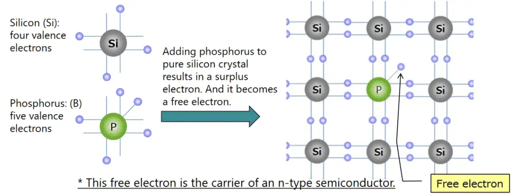
To produce N-type semiconductor material, the silicon semiconductor is doped with minute quantities of arsenic or phosphorus. Both of these elements consist of 5 electrons in their outer orbit. Since silicon only has four electrons in its outer orbit the fifth electron has no pair to bond with and is allowed to roam freely. This allows an electric current to be formed through the silicon semiconductor, hence forming an N-type material.
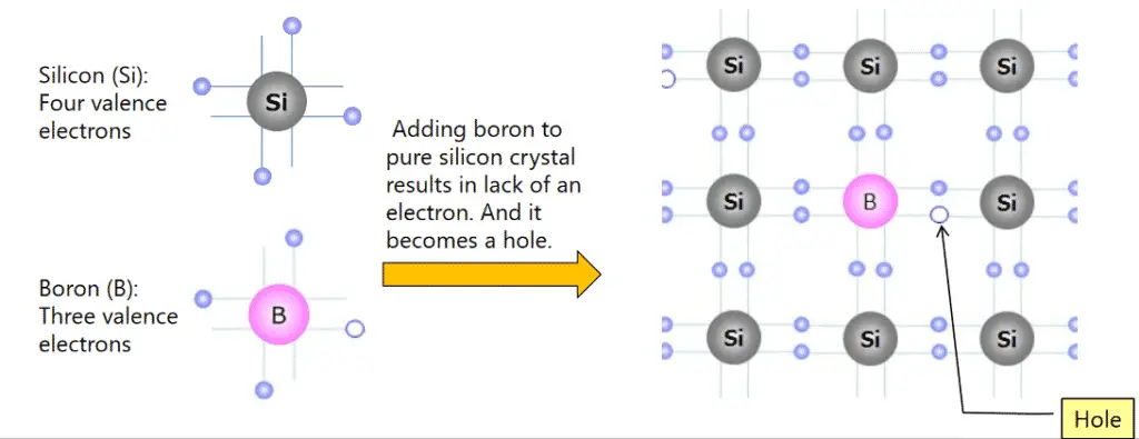
For p-type, the silicon is doped with either gallium or boron elements. Both of these elements have three electrons in their outer orbit. Hence when they are mixed with the silicon structure they form a hole in the valence band of silicon atoms. This mobile hole has a positive charge and moves in the opposite direction of electrons which are negatively charged. Due to the formation of positive holes in the silicon crystal lattice, these materials are known as p-type materials.
PN Junction Diodes
The most commonly used semiconductor diodes are the p-n junction diodes. p-n junction diodes are made by fusing p-type and n-type semiconductors. When both the semiconductors are fused a potential barrier voltage is created across the junction.
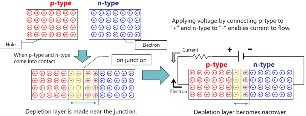
Figure 3. PN Junction Diode. Image credit: https://toshiba.semicon-storage.com
For this type of diodes, the N-type silicon semiconductor has an extra electron which is required by the p-type silicon. Therefore, the electrons migrate from the n-type material to the p-type material across the junction through the process of diffusion. Similarly, the p-type material has extra holes and the atoms on the n-type material require holes then the holes will diffuse into the n-type material across the junction. This process gives rise to the diffusion current formed across the junction. This process is repeated continuously until the number of electrons that have crossed the junction has a large electrical charge to either repel or allow any more charge carriers from passing over the junction.
Hence, a state of equilibrium is created which produces a potential barrier around the junction area. This is because the donor atoms are now repelling the holes and the acceptor atoms are now repelling the electrons. This potential barrier is a region of positive and negative charge on both sides of the junction is also known as the depletion layer. The depletion layer has no more free carriers compared to the semiconductor N-type and P-type materials.
To maintain a neutral charge around the junction area, the total charge on both the P and N-type semiconductors should be equal and opposite of one another. It can be observed from the diagram above that the depletion layer has a distance “D”. To maintain a neutral condition, the depletion layer would need to penetrate by a distance of Dp into the silicon from the positive side of the layer and Dn from the negative side of the depletion layer. This gives us a relation of Dp*NA = Dn*ND. By maintaining this relationship an equilibrium state can be acquired.
Operation of the P-N Junction Diode
The P-N junction diodes have two regions which are the P-type and N-type. The electrons will flow from the n-side to the p-side only when there is an increase in the voltage. Similarly, holes from the p-side will move to the n-side only when the voltage applied to the P-type material is increased. In simpler words, a push is required to move the electrons or holes to move from one side to another. This push creates a concentration gradient which allows the charge carriers to flow from an area of high concentration to an area of low concentration through the process of diffusion. This process allows current to flow in the circuit.
Biasing Conditions of P-N junction
Three types of biasing conditions can be obtained for p-n junctions when a voltage is applied. They are:
- Zero Bias in which no external voltage is applied.
- Forward Bias
- Reverse Bias
Forward Bias
In a forward bias condition, the positive terminal of the voltage potential or battery is connected to the p-type material and the negative terminal is connected to the n-type material. The anode is positive to the cathode.
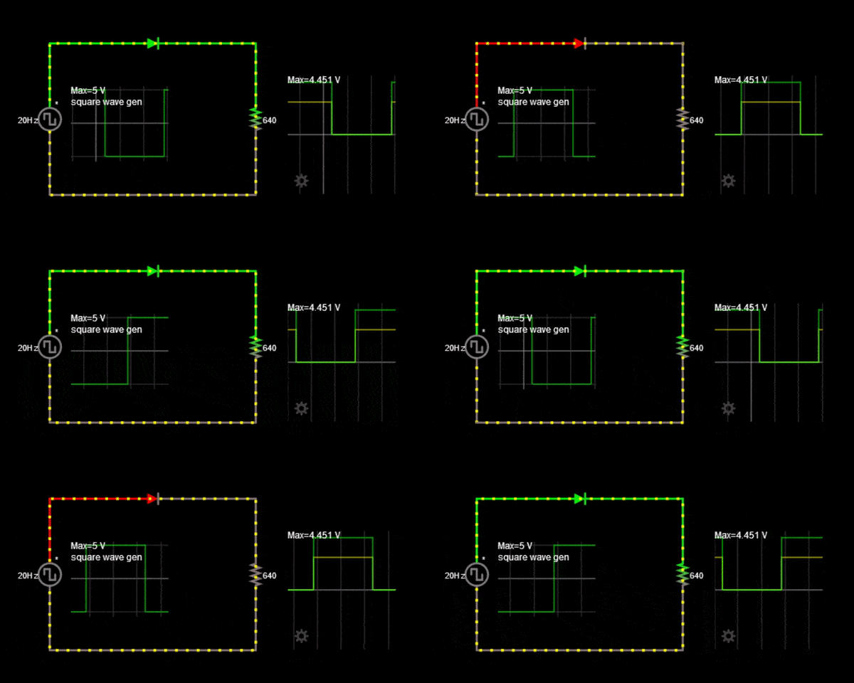
In a forward-biased condition, the built-in electric field and the external applied electric field are opposite to one another. When both the electric fields are added together the resultant electric field is much lesser in magnitude compared to the built-in electric field. This results in creating a less reactive depletion layer as well as reduces its size.
The resistance of the depletion layer becomes negligible when a large voltage is applied. If the semiconductor material is silicon, an applied voltage 0.6V voltage can result in the overall resistance of the depletion region becoming completely negligible. This allows the current to flow freely across the circuit without any obstructions.
Reverse Bias
The p-n junction is said to be reverse-biased when the positive terminal of the voltage potential is connected to the n-type material and the negative terminal is connected to the p-type material. The anode is negative to the cathode.
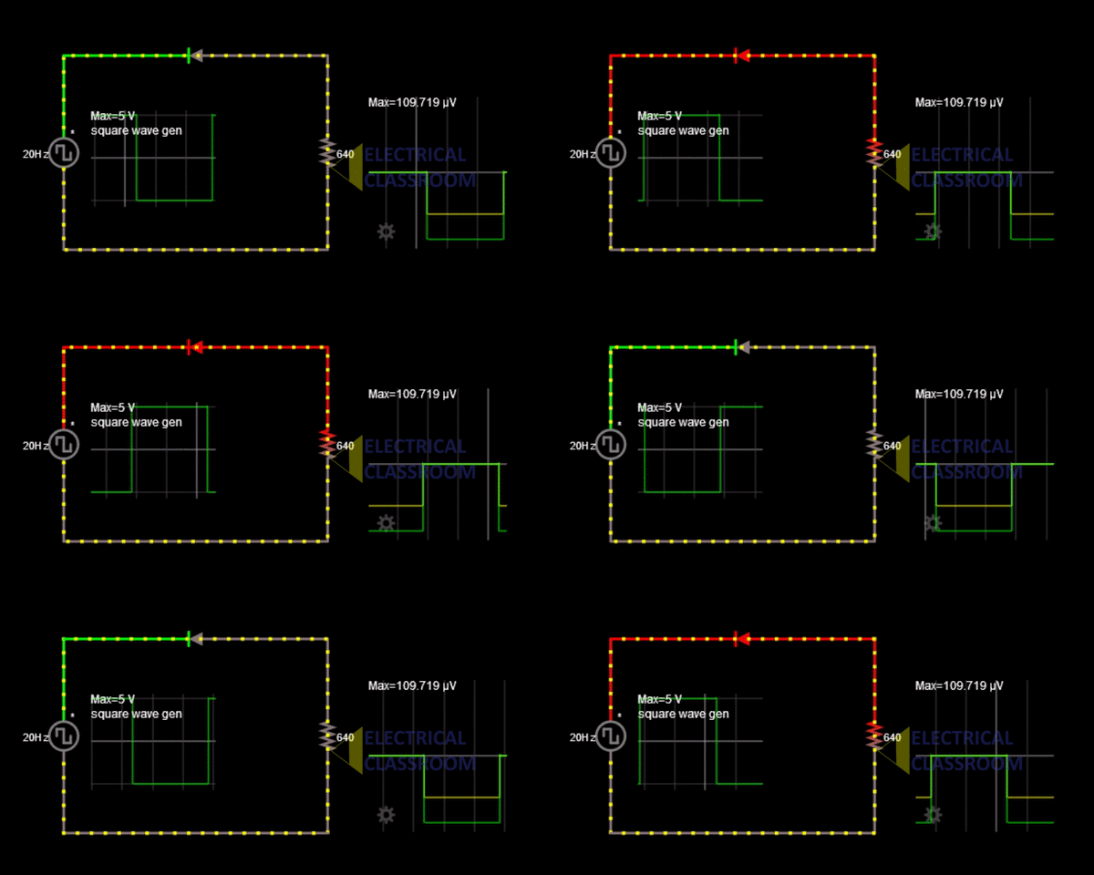
In a reverse biased condition, the built-in electric field and the applied electric field are in the same direction. When both the fields are added the resultant electric field is also in the same direction and is much more massive than the built-in electric field, therefore, creating a more resistive, thicker and larger depletion layer. As the voltage applied increases, the depletion layer would grow more resistive and thicker.
VI Characteristics of P-N Junction Diode
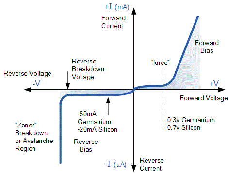
The VI characteristics of the PN junction diode are denoted by a curve that shows the relationship between the voltage and current in a circuit. Figure 6 shows the VI characteristics of the PN junction diode. From this curve, it can be seen that there are three operating regions in a diode. They are:
- Zero bias
- Forward bias
- Reverse bias
As discussed earlier, in a zero bias condition the circuit is not connected to any external voltage supply which would mean the potential barrier at the junction does not change therefore no current flows through the diode.
In the forward bias condition, an external voltage is applied to the diode. This allows current to flow through it as the potential barrier reduces in size and thickness. For silicon, the applied voltage needs to be around 0.7V and for germanium, it needs to be around 0.3V. It can be observed that when operated in forward bias condition, the current flow increases in the circuit, therefore, giving a non-linear relationship between current and voltage. This is because the voltage applied to the diode is overcoming the potential barrier to allow the current to flow through the junction. Once the barrier is overcome by the diode, the characteristics of the diode behave normally giving a linear graph.
Under the reverse bias condition the overall potential barrier thickness increases. It is observed that the reverse saturation current flows due to the minority carriers present in the junction. When the applied voltage is increased the minority carriers gain kinetic energy which affects the majority carriers. This can result in the diode breaking down or be destroyed altogether.
P-N Junction Diode Breakdown
Breakdown of P-N junction diodes occurs due to two phenomenon namely:
- Zener Breakdown
- Avalanche Breakdown
Zener Breakdown
This phenomenon is observed in a p-n junction diode which is heavily doped, has a thin junction and the width of the depletion layer will be small. Zener breakdowns do not damage them. The rise in current is also very minute and is caused due to the drifting of electrons.
Avalanche Breakdown
Avalanche breakdown occurs in the p-n junction which is not that heavily doped, has a thick junction and a depletion layer with a wider width. Avalanche breakdown occurs when a high reverse voltage is applied across the diode. The electric field across the junction will keep increasing as the applied reverse voltage is increased. Avalanche breakdowns are usually destructive.
Application of PN junction Diodes
PN junction diodes are known to be the basic building blocks of most of the semiconductor devices available including:
- It is also used for rectification in electric circuits. The process of rectification is converting alternating current to direct current. The p-n junction diode allows the current to flow when it is in its forward biased condition and blocks the current when it is in its reverse biased condition. These conditions allow it to be used as a rectifier.
- The diode is also for DC restoration in clamping circuits.
- It is also used for waved shaping in clipping circuits
- Diodes are used in demodulation circuits.
- They are used in voltage multipliers.
- P-N junction diodes are also used as a switch in digital logic circuits which are used in circuits.
- They are widely used for voltage regulation.
Summary
A diode is a semiconductor device made by fusing together p-type and n-type materials. It allows current flow in only one direction. When its anode is connected to positive and cathode is connected to negative it is said to be forward biased and allows current flow. When the anode and cathode are connected otherwise, it is said to be reverse biased. When the applied reverse bias voltage exceeds a certain level, avalanche breakdown occurs and the diode starts conducting in reverse biased condition.
